The Evolution of Printed Electronics and Sensor Technology: A Century of Progress
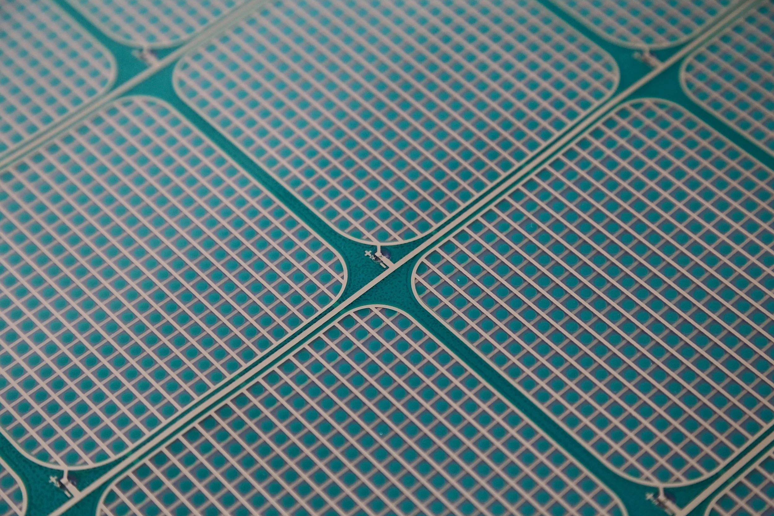
Close-up of Scanalytics patented smart flooring sensor system
Printed electronics and sensor technology have transformed the way we interact with the world around us. From the early 20th century to today's advanced wearables and smart flooring sensors, these technologies have continually evolved, bringing about unprecedented changes in various industries. This blog post delves into the history of printed electronics and sensor technology, highlighting key breakthroughs and their significant impacts.
Early Beginnings in the 20th Century
The origins of printed electronics can be traced back to the early 20th century when scientists and inventors began experimenting with conductive materials. In 1903, Albert Hanson, a German inventor, filed a patent for the first printed circuit. He used flat foil conductors laminated to an insulating board to create simple electronic circuits, laying the groundwork for future developments in the field.
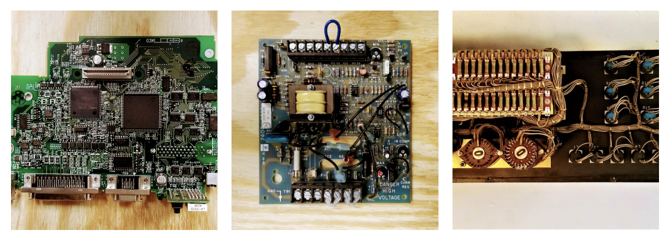
Printed Circuit Boards from the 1950s, 80s and 2000s (source: MRO Electric)
The 1920s and 1930s saw the rise of radio technology, which spurred interest in more compact and efficient electronic components. In 1936, Paul Eisler, an Austrian engineer, developed the first true printed circuit board (PCB) while working on a radio set. Eisler’s innovation allowed for more complex and reliable electronic devices, setting the stage for the modern electronics industry.
The Advent of Sensor Technology
Sensor technology also began to take shape in the early 20th century. In 1928, Dr. Herbert H. Einstein, a physicist, developed the first strain gauge, a device used to measure mechanical strain. This invention marked a significant step forward, enabling precise measurements in engineering and scientific applications.
During World War II, sensor technology saw significant advancements due to military needs. Pressure sensors, accelerometers, and temperature sensors were developed to improve the performance and reliability of military equipment. These early sensors were bulky and expensive, but they paved the way for the miniaturized, affordable sensors we use today.
Key Breakthroughs in the Mid-20th Century
The mid-20th century was a period of rapid progress in both printed electronics and sensor technology. In 1957, the launch of the Soviet satellite Sputnik spurred the United States to invest heavily in space exploration, leading to numerous technological advancements. NASA played a crucial role in the development of sensors and printed electronics during this era.
One notable example is the Apollo program in the 1960s, which required highly reliable sensors for navigation, life support, and communication systems. NASA developed various printed sensors for these applications, significantly advancing the field. These sensors were critical in ensuring the success of missions like Apollo 11, which landed the first humans on the Moon in 1969. Also important in this development was the emphasis on lightweight technology demanded by space exploration.
Texas Instruments, source: Texas History
Texas Instruments and the Rise of Microelectronics
Texas Instruments, founded in 1951, became a major player in the development of microelectronics and sensors. In 1958, Jack Kilby, an engineer at TI, invented the integrated circuit (IC), which revolutionized electronics by allowing thousands of transistors to be printed on a single chip. This innovation was crucial for the miniaturization and cost reduction of electronic devices.
In the 1970s and 1980s, TI continued to innovate in the field of sensors. They developed various types of sensors, including temperature, pressure, and motion sensors, which found applications in consumer electronics, automotive, and industrial sectors. TI’s contributions helped to make sensors more accessible and affordable, driving their widespread adoption.
Printed Electronics in the Late 20th Century
The late 20th century saw significant advancements in printed electronics, particularly with the development of flexible and wearable electronics. In the 1980s, researchers began exploring the use of conductive inks and flexible substrates to create lightweight, bendable electronic circuits. These innovations opened up new possibilities for integrating electronics into everyday objects.
One of the major breakthroughs in printed electronics came in the early 2000s with the development of organic electronics. These are electronic devices made from organic-based materials that can be printed onto flexible substrates using techniques like inkjet printing and screen printing. Organic light-emitting diodes (OLEDs) and organic photovoltaics (OPVs) are notable examples of this technology. Much of the manufacturing of this technology has now moved to China. Printed electronics became far more cost-effective than the development days of NASA, due to the scale and customer demand.
The OE-A, the Organic Printed Electronics Associations this ecosystem of suppliers, businesses and customers defining printed electronics as “flexible, organic and printed electronics stands for a revolutionary new type of electronics – also called “emerging electronics” – which is thin, lightweight, flexible, robust, and produced at low cost. “Emerging electronics” means electronics beyond the classic silicon approach, including flexible, printed electronics from organic, polymeric or inorganic materials. The organic and printed electronics technology also enables a wide range of electrical components to be produced and can be directly integrated into low cost reel-to-reel processes. This enables single-use, ubiquitous electronic devices and new applications.” (Source: OE-A)
The Rise of Wearables and Smart Devices
The 21st century has witnessed the rapid growth of wearable technology, which heavily relies on printed electronics and advanced sensors. Wearable devices, such as fitness trackers, smartwatches, and health monitors, have become increasingly popular due to their ability to provide real-time data and personalized insights. Flexibility and thin profiles were critical in the advancement of wearable technology.
For instance, fitness trackers like those made by Fitbit and Apple incorporate multiple sensors, including accelerometers, heart rate monitors, and GPS, to track physical activity and health metrics. These sensors are often printed onto flexible circuits, allowing the devices to be lightweight and comfortable to wear.
Source: Slate
Other applications: Hollywood and Healthcare
Pixar and other entertainment companies utilized wearables for motion capture. Actors wear sensor devices to capture facial expressions and natural movement that could later animated to create more fluid, natural characters. There are medical applications, for example blood pressure monitoring devices and administrative applications, kiosks at check in for labs and hospitals.
Space Exploration and the Future of Printed Electronics
NASA continues to be at the forefront of printed electronics and sensor technology. One example is the development of flexible sensors for space suits. These sensors can monitor astronauts' vital signs and environmental conditions, ensuring their safety during space missions. The flexibility and durability of printed sensors make them ideal for the harsh conditions of space.
In addition, NASA has been exploring the use of 3D printing to create electronic components and sensors directly on spacecraft. This approach could significantly reduce the weight and cost of space missions, as well as enable on-demand production of parts in space.
Benefits of Printed Electronics
Printed electronics offer numerous advantages over traditional electronics, including:
Cost-Effectiveness: Printing electronic components is generally cheaper than traditional manufacturing methods, making electronics more affordable.
Flexibility: Printed electronics can be made on flexible substrates, allowing for the creation of bendable and wearable devices.
Lightweight and Thin: Printed components are often lighter and thinner than their traditional counterparts, which is beneficial for applications like wearables and portable devices.
Scalability: Printing techniques can be easily scaled up for mass production, enabling the widespread adoption of electronic devices.
Customization: Printed electronics can be customized for specific applications, providing greater versatility in design and functionality.
Conclusion: The Future of Smart Flooring and Scanalytics
As we look to the future, the integration of printed electronics and sensor technology into everyday objects continues to expand. “Smart flooring is the perfect fit for printed electronics. It demands a flat surface, a lot of sensors, and a low cost at scale.” - Dr. Gene Chen, VP of Hardware and Process. One exciting development is smart flooring, which incorporates sensors to monitor and analyze foot traffic, detect falls, and enhance energy efficiency. Companies like Scanalytics are leading the way in this field, using printed sensors to create intelligent flooring systems that provide valuable data for building management and safety. As Scanalytics continues to evolve its product, it looks to print on “green” plastics, meaning ones with biodegradable materials and to explore alternative inks. Silver ink is the predominant ingredient today due to its conductive properties yet there are also organic-based inks and other Earth elements that are conductive and also more abundant such as copper and aluminum.
In conclusion, the history of printed electronics and sensor technology is a testament to human ingenuity and innovation. From early experiments with conductive materials to the development of advanced wearables and smart flooring, these technologies have revolutionized various industries and improved our daily lives. As we continue to push the boundaries of what is possible, the future of printed electronics and sensors promises to be even more exciting and transformative.


